
Product Development
Connected embedded products don’t always need to start from scratch. Fairfield Technology combines practical engineering experience with reusable hardware and software to accelerate development, reduce technical risk and provide a proven foundation for your product.
The approach used throughout product development reflects Fairfield Technology’s broader design philosophy, with an emphasis on reducing risk, keeping designs practical, and considering hardware and firmware together from the outset.
A typical development process follows three stages:
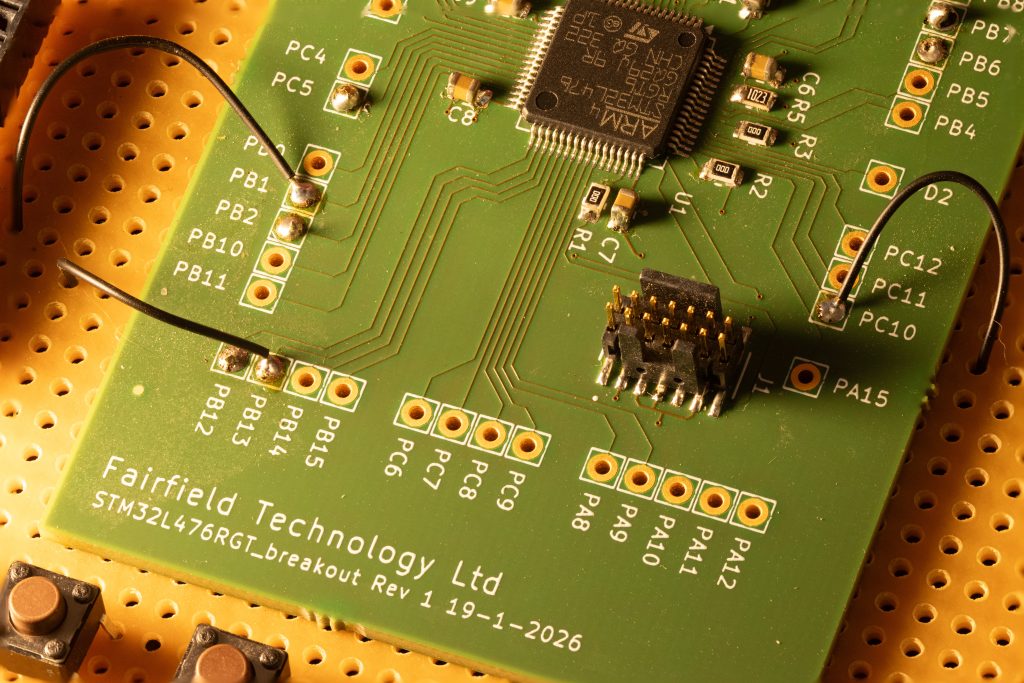
Investigate & de-risk
1. Requirements and system design
The project requirements are reviewed and developed into a practical system design, considering hardware, firmware and communications together from the outset. Key technical decisions and areas of uncertainty are identified early.
2. Technology and component evaluation
Suitable technologies and components are investigated and evaluated, using manufacturers’ development kits and evaluation boards where appropriate. This allows important design choices to be tested before committing them to custom hardware.
3. Technical investigation and de-risking
Where a particular part of the design requires further investigation, focused prototypes or custom investigation PCBs can be developed to evaluate it in more realistic conditions. Measurements and practical testing are used to understand limitations, verify assumptions and reduce technical risk before the main design proceeds.
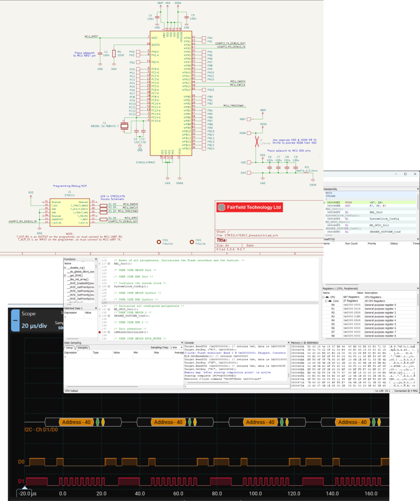
Develop & prove
1. KiCad schematic & PCB design using reusable KiCad libraries and design blocks
KiCad is a modern, well supported PCB design package that is seeing increased uptake. It is open source software so the customer can take the PCB design from Fairfield and continue work on it with no investment.
2. Embedded firmware development using reusable firmware components where possible
Fairfield continually develops and maintains a reusable codebase that can be incorporated into customer projects where appropriate. Using proven software for common, low-level functionality reduces development time and allows effort to be focused on the requirements unique to the product. Fairfield’s reusable components can be provided under licence, while project-specific software developed for the customer is owned by the customer.
3. Debugging and bring-up
– including using SEGGER tools (J-Link and Ozone debugger and performance analyser) where appropriate.
4. System testing & verification
Hardware, firmware and communications are tested together as a complete system against the agreed requirements. Appropriate test equipment and diagnostic tools are used to verify correct operation, investigate edge cases and identify problems before the design progresses towards production. Small PC applications can be created to assist in monitoring and configuring designs.
Complete & refine
1. Final testing and refinement
Any issues identified during system testing are resolved and the design refined as necessary before completion.
2. Project handover
On completion, the project is handed over to the customer together with the agreed design files, source code and other project deliverables, leaving the customer in control of their product.
3. Further development when required
Fairfield may remain available for subsequent changes, enhancements or further development where required, without making ongoing support an assumed part of every project.
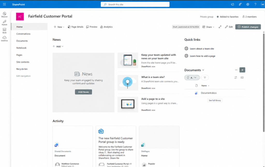
4. Customer project portal (coming soon)
Customers will have access to a dedicated SharePoint project portal providing a central location for project files, deliverables and other agreed information.